I did not mention the term "decimation" yet at all because it is neither a process nor is it mystic - it's trivial. It is required when a bitstream, e.g. the output of an analogue modulator, shall be converted to a PCM signal.
The core statement is: Without losing any information in oversampled signals as many samples can be left out until the signal is not oversampled any more. (That's why it is called "oversampled"!)
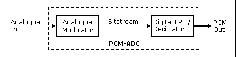
Figure 11 - Delta Sigma based ADC with PCM Output
Decimation takes place in delta sigma converters at the output of the digital low-pass filter. The bitstream is clocked with the sampling rate times the oversampling rate (e.g. 64 times the sample rate), and so the output of the digital low pass is clocked with the oversampling rate, too. But the sample rate clock (twice the input bandwidth) is required at the digital output only. Here decimation comes up: For an oversampling rate of e.g. 64 every 64th sample is taken, all others are discarded. This is possible because the signal is bandwidth limited by the digital low pass filter correspondingly. Quite simple - isn't it?
Multi-Bit ConverterThe feedback from the 1-Bit DAC to the block "Difference" introduces a lot of noise in an analogue modulator like in Figure 2. It is possible to reduce this noise by not only using one, but several bits instead. The comparator of Figure 2, which actually operates as a 1-bit ADC, is replaced by an N-bit ADC, and the latch and the DAC must be N bit wide, too:
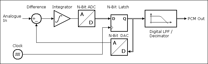
Figure 12 - Delta-Sigma based Multi-Bit ADC with PCM Output
The modulator's output signal will also become N bit wide and thus can no longer be called "bitstream", but it is as suitable to be converted to a PCM signal as the single bit wide bitstream is. Because less noise is introduced, the oversampling rate may be reduced or the PCM output's width can be increased. This is why in practice multi-bit modulators are normally used in ADCs. Note: The modulator's internal signal width "N" is usually a few bits only.
Mathematical Operations with Bitstream SignalsDoing mathematical operations like adding two signals or multiplying a signal with a constant (or with another signal) or even other linear or nonlinear operations like filtering is easy to understand for PCM signals. But how to do this with bitstream signals? Any non-trivial mathematical operation on quantized signals significantly affects the lower significant data bits but a bitstream has no LSBits. The input is a one-bit signal and the output has to be a one-bit signal, too!
The first approach is obvious, but not very smart: Convert the bitstream to a PCM signal, do the desired operation(s) and convert the result back to a bitstream:
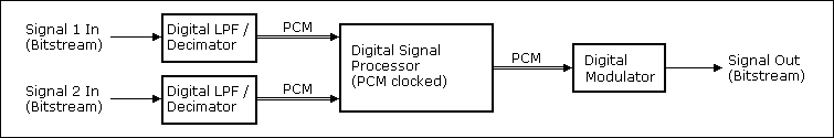
Figure 13 - Bitstream Operations using the PCM Detour
In practice, the digital signal processor in this block diagram may be a simple adder or multplier circuit. Also, there must not necessarily be a second bitstream input.
This "less smart" method takes one digital filter/decimator per input signal and one digital modulator for the output signal. Another issue of this method is the PCM clock (or sample rate resp.) which has to be introduced: A bitstream has no other sample rate than its bitstream clock, so that an arbitrary PCM sample rate ought to be chosen. This causes a loss of signal bandwidth due to the required digital filter and decimator.
The second approach is a more clever way to do it: For example, what happens if you want to just add two bitstream signals (e.g., mix two audio signals) and simply add the bits of both bitstreams? You'll get a 2-bit signal (PCM, this not what you need), but its average level still represents the sum of the original input signals. We "only" need to convert this 2-bit PCM signal into a 1-bit one. Just one digital modulator is needed for that, not more, not less:
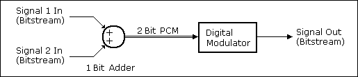
Figure 14 - Adding two Bitstream Signals
To understand this, we need a closer look on the digital modulator I explained in Figure 3. What I did not point out there is the fact that
Actually, the subtractor "Difference" in Figure 3 operates at the bitstream's clock rate and subtracts the 1-Bit DDC's PCM output signal from another, slowly clocked PCM signal. This subtractor is also able to subtract two PCM signals, both with the higher clock rate, of course. While the 2-bit sum of both bitstreams is not a usual PCM signal that represents the actual signal value at any time, it still can be viewed as a usable PCM signal for the digital modulator because it is sufficient when its temporal average value is correct. This, BTW, is very similar to the situation with the multi-bit signals in multi-bit converters.
Because the digital modulator's signal with needs only to be as wide as its digital input, in this example the circuit diagram for the digital modulator becomes quite simple as the bitstream adder's output signal is only 2 bit wide.
The general solution for mathematics with bitstreams looks like this:
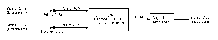
Figure 15 - Bitstream Operations Directly on Bitstream Signals
That's it. This "smart" solution takes no digital filter/decimator per input signal and only one (often quite simple) digital modulator for the output signal.
Additional Thoughts and CognitionsAlias effects: Delta sigma converters must run with sampling frequencies much higher than twice the maximum signal frequency (which is the minimum sample frequency of e.g. digital outputs). This has a very welcome consequence on alias effects: Only input signal frequencies close to the sampling frequency will be folded back and can cause alias signals as you can see in the graphic below:
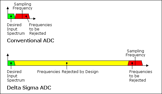
Figure 16 - Distances of Desired and Alias Frequency Bands
Thus it becomes obvious that conventional ADCs need expensive low pass filters in order to obtain a bandwidth close to the theoretical Nyquist limit. Delta sigma converters require simple RC low pass filters only and with a little more expense for a 2nd order filter one will get a virtually ideal behaviour. On the other hand an output low pass filter preceeding the decimator is required, which again can be realized more precisely, easily and cheap in digital techniques. Note that in practice the proportions are much more extreme than in the graphic above as due to limited space an oversampling rate of approx. 16 only is shown there.
DACs: The input signals of DACs are bandwidth limited by nature, so an input low pass filter is not necessary (it already had to be present when the digital signal was produced). An analog output filter is required anyway to suppress high frequency noise.
Infinite resolution of the bitstream: In analogue modulators the bitstream is sampled, but not quantized. It still has an infinite resolution just like the analogue signal has. It is superimposed by noise of course, but the more noise you filter out (the lower the low pass filter's frequency limit is), the more of the original resolution is usable - (theoretically) without limitation. This fact is also exploited by:
Direct Stream Digital (DSD) based devices: Traditionally digital devices use numerical representations of analogue samples, PCM in case of a serial signal. Delta sigma ADCs and DACs gain the PCM data out of the bitstream data (and vice versa) which is already a digital signal by means of low pass filters.
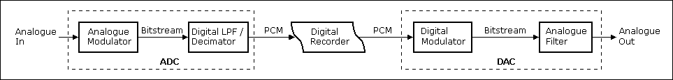
Figure 17 - Complete Delta Sigma Based PCM System: 2 Delta Sigma Converters
Why not record the bitstream directly? Conversion in delta sigma ADCs and DACs is executed in two steps each and as always each step has negative effects on the signal quality. Leaving out half of these steps - the filter in the ADC and the modulator in the DACs - should improve the performance of the complete system. Both, the quantization noise due to the limited number of recorded PCM bits and the conversion noise of the digital modulator would be dropped.

Figure 18 - Complete Delta Sigma Based DSD System: 1 Delta Sigma Converter only
This is actually done on super audio CDs (SACDs). The whole system from the analogue input to the analogue output now requires only one modulator and one low pass filter instead of two of both required with conventional digital recording. Please remember: The bitstream of modern, high quality ADCs and DACs use an oversampling rate of 64, e.g. the amount of data is 64 bits for each audio sample - compared to 16 or up to 20 or 24 of conventional bits required for a comparable quality. Technically, SACDs are DVDs and based on a sampling frequency of 2.8224 MHz (= 2.8224 MBits net per channel). Not much that more than on audio CDs (0.7056 MBits net per channel), and no problem at all for a DVD with its high capcity.
Class-D Power Amplifiers:
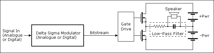
Figure 19 - Power Amplifiers using a Digital Output Stage
Both output transistors operate in push-pull mode, i. e., alternatingly one of both is conducting while the other one is switched off. Thus the bitstream is amplified to the high level of the power supply and is available at the output with low impedance. In order to regain the bitstream's mean value a simple LC-low-pass filter is sufficient in practice. A typical representative of this kind of amplifier is the LM4670, a simple and cheap low power amplifier with an analogue input, so simple that even the LC-low-pass filter is omitted and only the speaker's parasitic inductance remains as "low-pass filter". In contrast to that the TPA3200D1 is more complex, has higher output power and includes a digital (IIS-)input.
For the sake of completeness it shall be mentioned that for the operation of a class-D amplifier an analogue pulse width modulated (PWM) signal with a sufficiently high frequency can be used instead of the bitstream produced by a Delta Sigma converter. In contrast to digital pulse width modulated signals the pulse width ratios of analogue pulse width modulated signals are not quantized. With digital sources PWM operation does not suggest itself much, but with anlogue sources both techniques can be found in practice. In this case the pulse width modulator consists of a comparator comparing a triangle wave of e. g. a couple of MHz with the analogue input signal. An example is the TDA7490.
Compared to a conventional analogue class-AB amplifier, which advantages and disadvantages does such a class-D amplifier show?
In order to reduce both these disadvantages the supply voltage dependency as well as the output impedance can principally be lowered by degenerative feedback. But, if at all, this is by far not feasible in an amount as it is in analogue amplifieres as phase shifts inside the modulator and the low pass filter in conjunction with a degenerative feedback very soon lead to instabilities. Usually Delta Sigma amplifiers do not include degenerative feedback (as far as I experienced, at least). Once more, for the sake of completeness it shall be mentioned that PWM amplifiers do not incorporate phase shifting modulators so that degenerative feedback is much easier or much more efficient to achieve.
In analogue Delta Sigma based power amplifiers another trick is possible to drastically improve the signal quality:
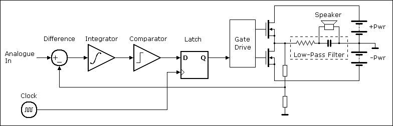
Figure 20 - Power Output Stage as Part of the Delta Sigma Modulator
Compare to Figure 2: Instead of feeding back the bitstream via a 1-bit DAC to build the difference in this case a portion of the power transistor's output is directly fed back. Thus it is guaranteed that independent of all parasitic effects like supply voltage variations or the transistor's resistances the mean value at the low-pass input is always exactly proportional to the analogue input signal. Excellent performance is feasible by this concept. An example for that is the AD1996. Unfortunately, this trick works for amplifiers with analogue inputs only.
Conclusion: Class-D power amplifiers offer a much higher efficiency and less exhaust heat at the expense of their signal quality. Thus they are favourable for generic public address systems, where high power, small size and probably portability too, are required. They are less predestinated for high-quality audio amplifiers. Constructively the most critical elements are the output transistors: The faster they switch, the less the losses are or the higher the switching frequency may be. The latter, on the other hand, allows low pass filters with higher frequencies, which due to their less phase shifts within the signal band allow stronger degenerative feedback, so that the signal quality can be improved. With the advancing semiconductor technology class-D amplifiers will be increasingly utilizable for high-quality audio amplifiers.
Delta Sigma Converters or Sigma Delta Converters? Mankind does not seem to agree on one notation. Both notations are used equally often when you search via Google. I decided to stay with that guy who told he is living in the Mississippi Delta, so deltas mean something to him - and for him only the Sigma River may have a Sigma Delta... good point. Later I found out that the original name "Delta Sigma" was coined by the inventors Inose and Yasuda and "Sigma Delta" is actually not correct. I was lucky...[From Uwe Beis ,Last update: August, 12th, 2007]
To Backward: An Introduction to Delta Sigma Converters (Delta-Sigma转换器 上篇)
Delta-Sigma原理一般应用在ADC应用中。具体来说,Delta-Sigma ADC的工作原理是由差动器、积分器和比较器构成调制器,它们一起构成一个反馈环路。调制器以大大高于模拟输入信号带宽的速率运行,以便提供过采样。模拟输入与反馈信号(误差信号)进行差动 (delta)比较。该比较产生的差动输出馈送到积分器(sigma)中。然后将积分器的输出馈送到比较器中。比较器的输出同时将反馈信号(误差信号)传送到差动器,而自身被馈送到数字滤波器中。这种反馈环路的目的是使反馈信号(误差信号)趋于零。比较器输出的结果就是1/0 流。该流如果1密度较高,则意味着模拟输入电压较高;反之,0密度较高,则意味着模拟输入电压较低。接着将1/0流馈送到数字滤波器中,该滤波器通过过采样与抽样,将1/0流从高速率、低精度位流转换成低速率、高精度数字输出。
简而言之,Delta就是差动,Sigma就是积分的意思。Delta-Sigma软件测试,我的理解应该是通过软件模拟差动积分的过程。具体来说,就是侦测外部输入的电压(或者电流)信号变化,然后通过软件积分运算,得出外部信号随时间变化的基本状况。
*博客内容为网友个人发布,仅代表博主个人观点,如有侵权请联系工作人员删除。