When looking for an introduction to delta sigma conversion I found that most explanations were from a very theoretical point of view. It took me a while to understand how Delta Sigma converters really work. So I decided to write this introduction for people who prefer circuit diagrams to reading abstract equations.
To understand what I'm talking about you should at least be familiar with:
- Standard analogue techniques (op-amps, comparators etc.)
- Standard digital techniques (latches, binary codes etc.)
- Standard ADCs and DACs (resolution, speed)
- What a low pass filter is (at least an analogue one)
- The sampling theorem (sample frequency > 2 x input bandwidth, alias effects)
Delta sigma converters are different from other converters. Note that I do not make a difference between analogue-to-digital (ADC) and digital-to-analogue converters (DAC). Both are very similar and what is realized in one of them using analogue signal processing circuitry is implemented in the other one using digital signal processing and vice versa. I will explain the delta sigma technique with the analogue-to-analogue delta sigma converter as the first object.
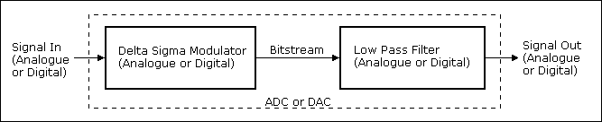
Figure 1 - Block Diagram of a Delta Sigma Converter
A delta sigma ADC or DAC always consists of a delta sigma modulator which produces the bitstream and a low pass filter.
The modulator will be implemented with digital technology if you have a digital signal source and in analogue technique in case of an analogue signal source. The same applies to the low pass filter: You will use an analogue low pass filter if you need an analogue signal output. A digital low pass filter will be implemented if you want a digital output. The digital low pass filter will probably be realized by a digital circuit or by an algorithm within a signal processor.
Before I proceed to the delta sigma modulator I would like to have a closer look to the bitstream and the low pass.
The Bitstream
The bitstream can be regarded either as a digital or an analogue signal. The bitstream is a one-bit serial signal with a bit rate much higher than the data rate e.g. of the ADC. Its major property is that its average level represents the average input signal level. A digital "high" represents the highest and a "low" represents the lowest possible output value.
- Analogue output: The bitstream will be converted to an analogue signal by a one bit DAC that converts the logic information (low / high or 0 / 1) to two precise analogue voltage levels, e.g. -1V and +1V.
- Digital output: A "high" (or "low" resp.) in the bitstream represents the highest (lowest) digital output value, e.g. hexadecimal FF (00) in an 8 bit system.
You can find a similar bitstream in a pulse width modulated (PWM) system but it has some disadvantages compared to the bitstream of a delta sigma modulator. The delta sigma kind of bitstream is also known as a pulse proportion modulated (PPM) signal. The serial transmission of numerically represented signal values (e.g. the serial output of a conventional ADC) is called pulse code modulation (PCM).
The Low Pass Filter
The low pass filter at the output is required, because you have to gain the average signal level out of the bitstream. You can regard the bitstream as a signal with its information in the lower frequency band and lots of noise above it. I presume low pass filters to be known and will not go into further deatils here.
The Delta Sigma Modulator
The delta sigma modulator is the core of delta sigma converters. As mentioned above it produces a bitstream. The average level of this bitstream represents the input signal level. A simple analogue first order delta sigma modulator block diagram looks like this:
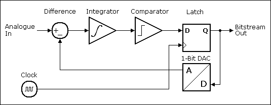
Figure 2 - Block Diagram of a First Order Analogue Delta Sigma Modulator
Please notice that due to the negative feedback loop the average(!) output level at the 1-Bit DAC must always be equal to the input signal level.
The digital counterpart looks just as simple:
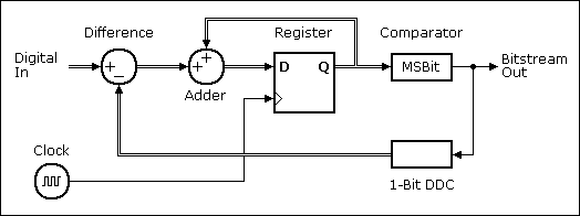
Figure 3 - Block Diagram of a First Order Digital Delta Sigma Modulator
The comparator, just like in the analogue version, decides whether its input value is higher or lower than a certain threshold and puts out a single bit signal, the bitstrem. BTW, due to the preceding integrator this threshold is arbitrary. In order to obtain the bitstream in the digital modulator it is sufficient to strip off the comparator's input MSBit.
A 1-Bit DAC can output two different values only. They are termed VRef- and VRef+ and those of the 1-Bit DDC (digital-to-digital converter) DRef- and DRef+ correspondingly. In both types of modulators they determine its input range. Examples:
In the analogue modulator input ranges result out of the reference voltages as follows:
| VRef- |
VRef+ |
Input Range |
| 0 V |
+1 V |
0 to +1 V |
| -10 V |
+10 V |
-10 V to +10 V |
Likewise, in the digital modulator the following input ranges are obtained:
| DRef- |
DRef+ |
Input Range |
Type |
| 00 (hex) |
FF (hex) |
00 (hex) to FF (hex) |
Unsigned Binary Byte |
| 8000 (hex) |
7FFF (hex) |
-32768 to +32767 (decimal) |
Signed Binary 16 Bit |
As a circuit diagram, the 1-Bit DDC may be as simple as a manifold of the input signal to all output data bits:
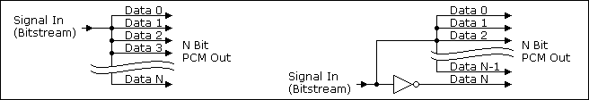
Figure 4 - Two simple 1-Bit DDCs
Left: Unsigned (0 to 2
n), Right: Signed (-2
n-1 to +2
n-1-1)
The first order modulator's signal diagrams look like this (analogue version):
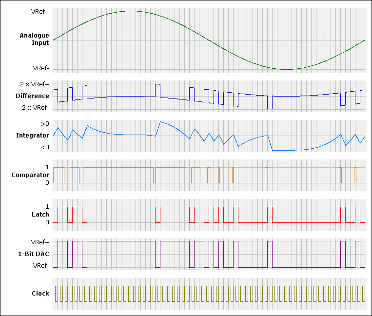
Figure 5 - Signals within a First Order Analogue Modulator
Note that in this example the clock rate, which here is also the sample rate, is 64 times higher than the frequency of the input signal. Conventional converters require a sample rate of more than twice the highest input frequency. Delta sigma converters require much more in order to produce a sufficient number of bitstream pulses. It is obvious: The more bitstream pulses are produced the better is the approximation of the input signal by the average bitstream.
Once again: The average (low pass filtered) bitstream never(!) exactly represents the input signal. It is always(!) superimposed by some kind of noise.
One way to reduce this noise is to further increase the clock rate. Due to the sampling theorem the sampling rate must be higher than twice the maximum input frequency. Any further increase is called "oversampling rate". Example: Assume an audio signal with a bandwidth of up to 20 kHz (and probably slightly more). A typical sampling rate (for DAT etc.) is 48 kHz. In a typical delta sigma converter the clock frequency (which usually is also the sample rate) will be 64 x 48 kHz = 3072 kHz. This is equal to an oversampling rate of 64. In the example above (Figure 4) the clock frequency is 64 times higher than the frequency of the input signal. This means that the oversampling rate must be less than 32 for the given input frequency. (I don't know why only oversampling rates in the form of 2n are actually implemented. In my opinion any other form of this factor should be possible, too.)
Another - and better - way to reduce the noise is to use a higher order delta sigma modulator. Bitstreams produced by higher order modulators produce less noise at the low pass filter outputs. Normally this noise is random. First order modulators show some strong frequencies in the power spectrum (non-random noise or residual tones), which is disadvantgeous. If the input signal is close to the limits of the input range this effect is worst with first order modulators. If you want to know more about this refer to "First Order Delta Sigma Modulator Disadvantages".
A second order delta sigma modulator may look like this:
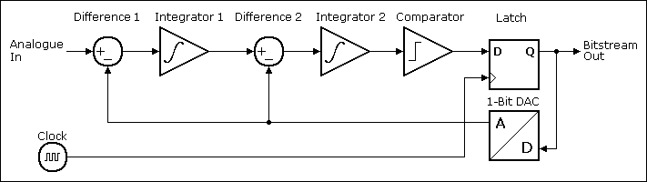
Figure 6 - Block Diagram of a Second Order Analogue Delta Sigma Modulator
The bitstream of such a modulator is much closer to the ideal pulse proportion signal than the one above so that
- either the input signal bandwidth may be higher,
- or the clock rate may be lower,
- or the output precision is increased (less noise)
whatever you want to achieve. Additionally "non-random noise" is avoided to a great extent.
Delta sigma modulators of orders higher than 2 are possible to construct but they cannot simply be made by adding further stages as above. The reason is that the phase turn caused by more than two integrators will make the system unstable. Low pass filters are used instead. Delta sigma ADCs for audio applications typically use 5th order modulators and, as mentioned above, oversampling rates of 64. The architecture may look different, e.g. 2-bit DACs, but the basic principle of operation remains the same.
5th order and an oversampling rate of 64 - why that much?
A Short Introduction to ADC and DAC Noise
As already mentioned within the average (low pass filtered) bitstream noise always remains. The amount of noise depends on a) the oversampling rate and b) the order of the modulator that produced the bitstream. Obviously it will not make sense to provide a 16 bit output to an ADC where the low 8 bit randomly change due to the remaining noise.
You may have heard that signals converted by ADCs suffer from quantization noise. Where does this come from? If a DC-voltage is applied to an ADC the output remains stable. It represents the input voltage more or less precisely, but without noise. So, where is there noise?
It's because the conversion is "more or less precisely" only. A constant error in a DC measurement corresponds to a random error or white noise (= noise with equal distribution over its spectrum) in a conversion with a varying signal (AC). A digital n bit signal can only settle to 2n values but the analogue input signal may have any value. It is this difference between the analogue value and its digital representation which causes the problem. This is called the quantization noise. In the example below a 4 bit ADC (= 24 = 16 quantization levels) is assumed:
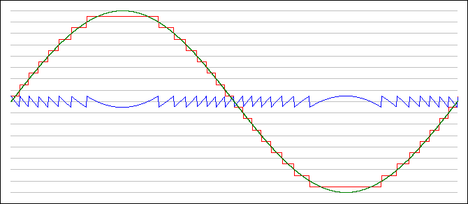
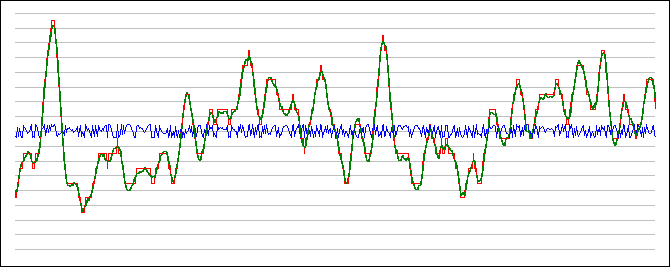
Figure 7 - Quantization Noise in Digital (PCM) Systems, Sinewave and Audio Signal
One can see that more quantization levels reduce the remaining quantization noise. Using an ideal ADC with n bits the signal to noise ratio (SNR) is:
n * 6.02 + 1.76 [dB] (or 2n * Sqr(3/2)) referred to a full scale sine wave signal or
n * 6.02 + 10.79 [dB] (or 2n * Sqr(12)) referred to the maximum peak-to-peak output voltage.
Thus for an ideal 16 bit ADC the SNR achievable is 98.1 dB and the SNR for the 4-bit signal above is 25.8 dB.
The Conversion Noise of Delta Sigma Converters
Please note that conversion noise and not quantization noise is discussed here. Conversion noise appears already in the bitstream. Quantization noise appears only when signals are represented digitally. As mentioned above the amount of conversion noise depends on the oversampling rate and the order of the modulator. It can be expressed mathematically and results in the following graphs for delta sigma modulators with orders of 0, 1, 2, 3, 4 and 5:
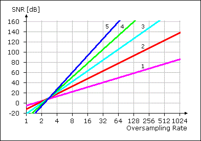
Figure 8 - Delta Sigma Conversion Noise
SNR vs. Oversampling Rate and Modulator Order (0 - 5)
Now you can figure out which parameters (oversampling rate and order) of the modulator are required to obtain which noise. If a signal must be quantized, you may decide either the quantization noise or the conversion noise to be the bottle neck of the overall noise performance. In case that both shall have an equal effect, the overall SNR is reduced by 3 dB related to each of the noise portions.
Example: A 16 bit ADC, realized with a 3rd order modulator and a 64 fold oversampling rate would add -106 dB of conversion noise to the -98 dB quantization noise, so that quantization noise is prevailing and will be deteriorated by less than 1 dB only.
These SNR-figures are valid only for ideal converters. As so often in practice, the actually yielded SNR amongst others depends on the conversion speed and the IC-technology.
High quality ADCs for audio applications provide 24 output bits. They use 5th order modulators so that the conversion noise could be theoretically at -160 dB. The quantization noise of a 24 bit converter could become better than -147 dB. Real good ADC achieve "just" 120 dB SNR (19.6 effective bits) due to the non-ideal operation of the modulator (Example: Cirrus Logic CS5381). Nevertheless 120 dB is a fantastic value: 106 or 1:1,000,000 is close to the dynamic range of the human ear! Another 24 bit delta sigma ADC I know yields an SNR of 140 dB, but with an output rate of 7 Hz "only" (Linear Technology LTC2440).
The "Noise View" on Delta Sigma Converters
The "conventional" way to explain Delta Sigma Converters is to look at the noise generated within the modulator and then to figure out how much noise remains after the low pass filter. This did not help me to understand what's going on inside the converters and so I disregarded this kind of view as yet. Let us have a short look on the mathematical background even though:
I want to describe the frequency response of a 1st order modulator like the one in Figure 2. But how to do it, when there are such strange, non-linear elements like comparators and latches in it? It took me a while to accept: The comparator/latch combination can be taken as an adder of noise to the output signal of the integrator, so a modulator block diagram like this results:
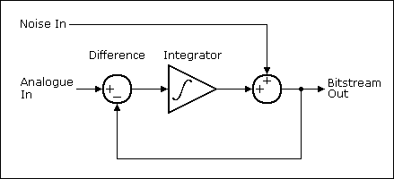
Figure 9 - Equivalent Circuit Block Diagram for Noise Considerations
It can be regarded this way because a) the output of the modulator still contains the average input value and b) the (mainly randomly) "jumping" bitstream is a kind of noise - white noise to be more precise. Think about this or just believe me.
The frequency responses from both inputs to the bitstream output result from the integrator being
- in the forward path of the loop for the analogue input so that a low-pass filter characteristic must result and
- in the feed-back path of the loop for the noise input so that a high-pass filter characteristic must result
We can compute both frequency responses which for 1st and 2nd order modulators look like this:
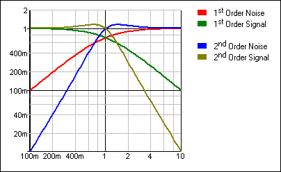
Figure 10 - Frequency Responses Causing Noise Shaping
In the lower frequency band the desired input signals are passed and changed little, while the noise is suppressed to a great extent. With higher order modulators the noise is even more suppressed. This is called "noise shaping". And this is the reason why higher order modulators produce less output noise.
If you now start to compute noise figures depending on the modulators order and the oversampling rate you will get the SNR-diagram shown in Figure 7. For further details refer to the Intersil application note "A Brief Introduction to Sigma Delta Conversion". (Attention: Figure 6 "SNR vs Oversampling Ratio" is wrong. Use "my" Figure 7 instead.) I found another interesting introduction for various kinds of A/D converters including delta sigma:The Rane company: Digital Dharma of Audio A/D Converters.